- 您现在的位置:买卖IC网 > Sheet目录415 > FDC3512_F095 (Fairchild Semiconductor)MOSFET N-CH 80V 3A 6-SSOT
�� �
�
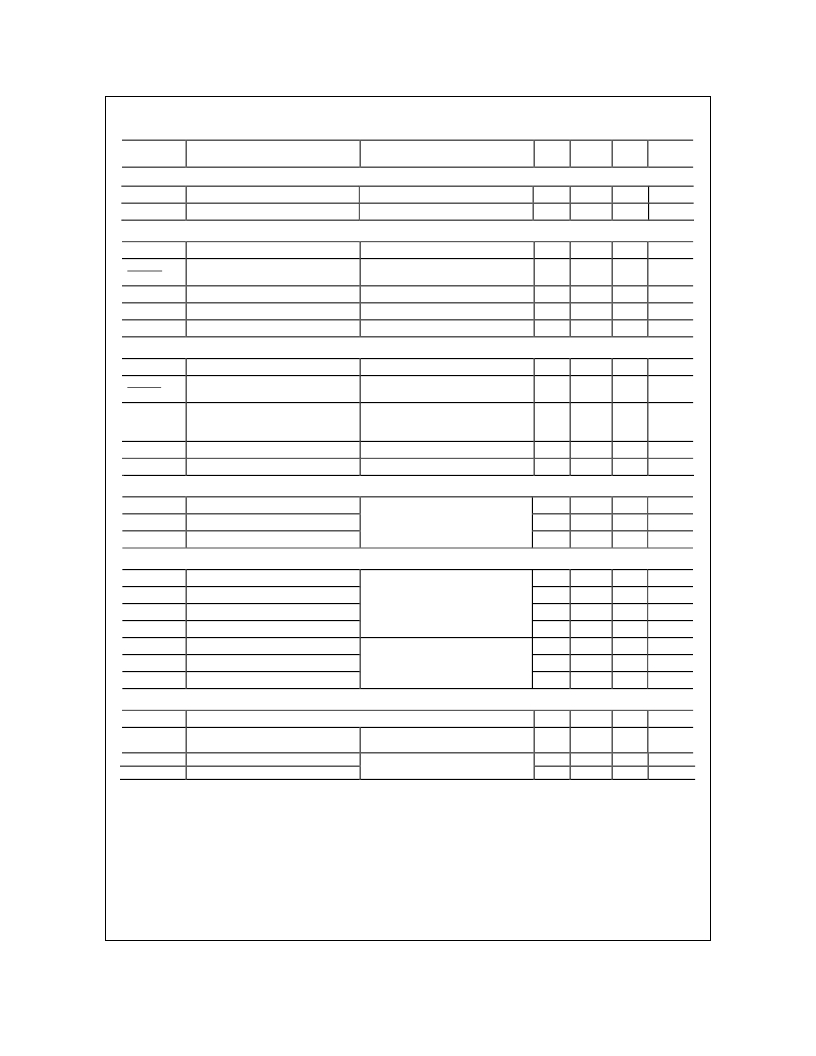
�Electrical� Characteristics�
�T� A� =� 25°C� unless� otherwise� noted�
�Symbol�
�Parameter�
�Test� Conditions�
�Min�
�Typ�
�Max� Units�
�Drain-Source� Avalanche� Ratings� (Note� 2)�
�W� DSS�
�I� AR�
�Drain-Source� Avalanche� Energy�
�Drain-Source� Avalanche� Current�
�Single Pulse, V� DD� = 40 V, I� D� =3.0 A�
�90�
�3.0�
�mJ�
�A�
�Off� Characteristics�
�BV� DSS�
�?� BV� DSS�
�?� T� J�
�I� DSS�
�I� GSSF�
�I� GSSR�
�Drain–Source� Breakdown� Voltage�
�Breakdown� Voltage� Temperature�
�Coefficient�
�Zero� Gate� Voltage� Drain� Current�
�Gate–Body� Leakage,� Forward�
�Gate–Body� Leakage,� Reverse�
�V� GS� =� 0� V,� I� D� =� 250� μ� A�
�I� D� =� 250� μ� A,� Referenced� to� 25� °� C�
�V� DS� =� 64� V,� V� GS� =� 0� V�
�V� GS� =� 20� V,� V� DS� =� 0� V�
�V� GS� =� –20� V,� V� DS� =� 0� V�
�80�
�80�
�1�
�100�
�–100�
�V�
�mV/� °� C�
�μ� A�
�nA�
�nA�
�On� Characteristics�
�(Note� 2)�
�V� GS(th)�
�?� V� GS(th)�
�?� T� J�
�R� DS(on)�
�I� D(on)�
�g� FS�
�Gate� Threshold� Voltage�
�Gate� Threshold� Voltage�
�Temperature� Coefficient�
�Static� Drain–Source�
�On� Resistance�
�On–State� Drain� Current�
�Forward� Transconductance�
�V� DS� =� V� GS� ,� I� D� =� 250� μ� A�
�I� D� =� 250� μ� A,� Referenced� to� 25� °� C�
�V� GS� =� 10� V,� I� D� =� 3.0� A�
�V� GS� =� 6.0� V,� I� D� =� 2.8� A�
�V� GS� =� 10� V,� I� D� =� 3.0� A;T� J� =� 125� °� C�
�V� GS� =� 10� V,�
�V� DS� =� 5� V�
�V� DS� =� 10� V,� I� D� =� 3.0� A�
�2�
�10�
�2.4�
�–6�
�56�
�61�
�97�
�14�
�4�
�77�
�88�
�141�
�V�
�mV/� °� C�
�m� ?�
�A�
�S�
�Dynamic� Characteristics�
�C� iss�
�C� oss�
�C� rss�
�Input� Capacitance�
�Output� Capacitance�
�Reverse� Transfer� Capacitance�
�V� DS� =� 40� V,�
�f� =� 1.0� MHz�
�V� GS� =� 0� V,�
�634�
�58�
�28�
�pF�
�pF�
�pF�
�Switching� Characteristics�
�(Note� 2)�
�t� d(on)�
�t� r�
�t� d(off)�
�t� f�
�Q� g�
�Q� gs�
�Turn–On� Delay� Time�
�Turn–On� Rise� Time�
�Turn–Off� Delay� Time�
�Turn–Off� Fall� Time�
�Total� Gate� Charge�
�Gate–Source� Charge�
�V� DD� =� 40� V,�
�V� GS� =� 10� V,�
�V� DS� =� 40� V,�
�V� GS� =� 10� V�
�I� D� =� 1� A,�
�R� GEN� =� 6� ?�
�I� D� =� 3.0� A,�
�7�
�3�
�24�
�4�
�13�
�2.4�
�14�
�6�
�28�
�8�
�18�
�ns�
�ns�
�ns�
�ns�
�nC�
�nC�
�Q� gd�
�Gate–Drain� Charge�
�2.8�
�nC�
�Drain–Source� Diode� Characteristics� and� Maximum� Ratings�
�I� S�
�Maximum Continuous Drain–Sourc� e� Diode� Forward� Current�
�1.3�
�A�
�V� SD�
�t� rr�
�Q� rr�
�Drain–Source� Diode� Forward�
�Voltage�
�Diode� Reverse� Recovery� Time�
�Diode� Reverse� Recovery� Charge�
�V� GS� =� 0� V,� I� S� =� 1.3� A�
�I� F� =� 3.0� A,�
�d� iF� /d� t� =� 300� A/μs�
�(Note� 2)�
�(Note� 2)�
�0.8�
�28.2�
�48�
�1.2�
�V�
�nS�
�nC�
�Notes:�
�1.� R� θ� JA� is� the� sum� of� the� junction-to-case� and� case-to-ambient� resistance� where� the� case� thermal� reference� is� defined� as� the� solder� mounting� surface� of� the� drain�
�pins.� R� θ� JC� is� guaranteed� by� design� while� R� θ� CA� is� determined� by� the� user's� board� design.�
�78°C/W� when� mounted� on� a� 1in� pad� of� 2oz� copper� on� FR-4� board.�
�a.�
�b.�
�2�
�156°C/W� when� mounted� on� a� minimum� pad.�
�2.� Pulse� Test:� Pulse� Width� ≤� 300� μ� s,� Duty� Cycle� ≤� 2.0%�
�FDC3512� Rev� B2(W)�
�发布紧急采购,3分钟左右您将得到回复。
相关PDF资料
FDC3535
MOSFET P-CH 80V 6-SSOT
FDC3601N
MOSFET N-CH DUAL 100V SSOT-6
FDC3612_F095
MOSFET N-CH 100V 2.6A 6-SSOT
FDC365P
MOSFET P-CH 35V 4.3A 6-SSOT
FDC5612_F095
MOSFET N-CH 60V 4.3A 6-SSOT
FDC5614P_D87Z
MOSFET P-CH 60V 3A 6SSOT
FDC5661N_F085
MOSFET N-CH 60V 6-SSOT
FDC602P_F095
MOSFET P-CH 20V 5.5A 6SSOT
相关代理商/技术参数
FDC3535
功能描述:MOSFET MOSFET; -80V P-Chan PowerTrench
RoHS:否 制造商:STMicroelectronics 晶体管极性:N-Channel 汲极/源极击穿电压:650 V 闸/源击穿电压:25 V 漏极连续电流:130 A 电阻汲极/源极 RDS(导通):0.014 Ohms 配置:Single 最大工作温度: 安装风格:Through Hole 封装 / 箱体:Max247 封装:Tube
FDC3601N
功能描述:MOSFET Dual N-Ch 100V Spec Power Trench RoHS:否 制造商:STMicroelectronics 晶体管极性:N-Channel 汲极/源极击穿电压:650 V 闸/源击穿电压:25 V 漏极连续电流:130 A 电阻汲极/源极 RDS(导通):0.014 Ohms 配置:Single 最大工作温度: 安装风格:Through Hole 封装 / 箱体:Max247 封装:Tube
FDC3601N
制造商:Fairchild Semiconductor Corporation 功能描述:MOSFET
FDC3612
功能描述:MOSFET 100V NCh PowerTrench RoHS:否 制造商:STMicroelectronics 晶体管极性:N-Channel 汲极/源极击穿电压:650 V 闸/源击穿电压:25 V 漏极连续电流:130 A 电阻汲极/源极 RDS(导通):0.014 Ohms 配置:Single 最大工作温度: 安装风格:Through Hole 封装 / 箱体:Max247 封装:Tube
FDC3612
制造商:Fairchild Semiconductor Corporation 功能描述:MOSFET
FDC3612_F095
功能描述:MOSFET 100V 2.6A N-CH POWERTRENCH RoHS:否 制造商:STMicroelectronics 晶体管极性:N-Channel 汲极/源极击穿电压:650 V 闸/源击穿电压:25 V 漏极连续电流:130 A 电阻汲极/源极 RDS(导通):0.014 Ohms 配置:Single 最大工作温度: 安装风格:Through Hole 封装 / 箱体:Max247 封装:Tube
FDC3616N
功能描述:MOSFET 100V NCh PowerTrench RoHS:否 制造商:STMicroelectronics 晶体管极性:N-Channel 汲极/源极击穿电压:650 V 闸/源击穿电压:25 V 漏极连续电流:130 A 电阻汲极/源极 RDS(导通):0.014 Ohms 配置:Single 最大工作温度: 安装风格:Through Hole 封装 / 箱体:Max247 封装:Tube
FDC3616N
制造商:Fairchild Semiconductor Corporation 功能描述:MOSFET